Getting started with diy PCB's

Do you have a technical question that doesn't really fit a specific console? Want some general info on electronics, hacking, making cookies, etc? Here's the place to ask! Go nuts.

Moderator:Moderators

Post Reply
User avatar
blaze3927
Portablizer
Posts:1114
Joined:Mon Dec 08, 2008 6:14 am
360 GamerTag:notjames
Location:Australia
Contact:
Getting started with diy PCB's

Post by blaze3927 » Tue Aug 31, 2010 5:22 am

well hello, it appears i require assistance...as usual

im wanting to start building my own printed circuit boards. now typical of me i rushed ahead and bought a pcb etching kit from jaycar, where it provides instructions on manually etching your own board or using a "photocoated board".
for the photocoated board o i just print out my design on standard inkjet with plain paper and thats it?

or would it just be easier for me to manually etch the board?


and also

Whats a nice program (EAGLE?) that would be suitable for drawing up pcb's before testing them: the job i'm looking to start off with is building a board for programming attiny 24 chips solder free (after soldering resistor etc to board). this is as simple as 10 pin idc heaer, 1resistor, holes for chip to slot in etc.)


expect more questions soon :P
thanks
Australian Kaillera server
[url]hhttp://i56.tinypic.com/ncb0wi.gif[/url]

User avatar
Rekarp
Portablizer Extraordinaire
Posts:2163
Joined:Thu Dec 28, 2006 1:52 am
PSN Username:Lnghrn_
Steam ID:rekarp
Location:Austin, Tx
Contact:

Re: Getting started with diy PCB's

Post by Rekarp » Tue Aug 31, 2010 7:35 am

I design all my PCBs with FreePCB. There isn't a program that I know of that you can "test" a PCB before hand. Theres programs like LTSpice and Labview that allow testing a circuit though.

I personally never found etching a PCB by hand to be useful. A pre-punched prototype PCB works just as well and takes about the same amount of time to make and is much cheaper. For stuff that needs PCBs? I just use either BatchPCB or PCBcart, depending on quantity of boards.
The wood master

Image

"I was under the impression Mac owners don't actually USE their machines, they just parade them around trying to evangelize the masses."

User avatar
timmeh87
Senior Member
Posts:3047
Joined:Mon Nov 14, 2005 10:19 pm
Location:Ontario, Canada

Re: Getting started with diy PCB's

Post by timmeh87 » Tue Aug 31, 2010 10:37 am

The photosensitive boards have to be exposed with UV light using a image printed onto clear plastic. ("overhead transparencies"). Then you wash away the photoresist and continue etching as normal

I did it once and then decided to never do it again because I did not get good results. The photoresist stuff is annoying to expose, and its very fragile and prone to scratches which mess up your design.

Did you read all the directions that came with your kit?.... Did it come with the photosensitive board? What exactly is /in/ one of these kits? All you need is blank board and two cups of etching solution..

I create my design in eagle, then use a laser printer to print the FLIPPED (!) image onto PHOTO (!) paper, and iron it directly onto BARE (!) PCB. If you get the right paper/printer combo, you can get it to stick to the boards really well. I can get down to about 8mil traces reliably.

As for etching, follow this amazing tutorial for making your own cupric chloride. Ferric chloride is way too expensive.
http://members.optusnet.com.au/eseychel ... index.html" onclick="window.open(this.href);return false;

also, regarding "testing", eagle can do a DRC and ERC check on your board (read help file). Its pretty useful when your design gets complicated and usually catches a bunch of errors that you did not.
Image

"Linux is only free if your time is worthless"

User avatar
blaze3927
Portablizer
Posts:1114
Joined:Mon Dec 08, 2008 6:14 am
360 GamerTag:notjames
Location:Australia
Contact:

Re: Getting started with diy PCB's

Post by blaze3927 » Fri Sep 03, 2010 5:28 am

Thanks for the replies.
it comes with two satchels of etching soluton:
sodium persuphate (?)
and kemo something.
a photosensitive board. and three plain boards
and mixing bowl

so at this stage it'll seem the best option is to print my pcb onto photo paper (i've read that inkjet should work ok?). iron onto pcb.

and then from there use the etching solution instructions the kit came with.

cheers
Australian Kaillera server
[url]hhttp://i56.tinypic.com/ncb0wi.gif[/url]

User avatar
timmeh87
Senior Member
Posts:3047
Joined:Mon Nov 14, 2005 10:19 pm
Location:Ontario, Canada

Re: Getting started with diy PCB's

Post by timmeh87 » Fri Sep 03, 2010 10:30 am

Inkjet will definitely not work. I dont know where you heard that... Its called the toner-transfer, laser toner is the only thing that works.

http://gilmore2.chem.northwestern.edu/p ... z2_prj.php" onclick="window.open(this.href);return false;
Image

"Linux is only free if your time is worthless"

Snow_Cat
Posts:463
Joined:Fri Aug 13, 2010 12:40 pm
Steam ID:Snow_Cat
Location:Here
Contact:

Re: Getting started with diy PCB's

Post by Snow_Cat » Sat Sep 04, 2010 12:27 pm

Nest of links. I could have also hit up instructables.com, hackedgadgets.com, makezine.com, hacknmod.com, elecktor.com... and others, but then this list would have been huge (nevermind that I deliberately did not include information on soldering, masking, drilling, milling, populating...)

User avatar
blaze3927
Portablizer
Posts:1114
Joined:Mon Dec 08, 2008 6:14 am
360 GamerTag:notjames
Location:Australia
Contact:

Re: Getting started with diy PCB's

Post by blaze3927 » Sat Sep 04, 2010 6:48 pm

Wow cheers guys,
so I think my best option is to print out a negative with my inkjet, then use works laser photocopier so i get the laser print of the board design onto the shiny side of matte photo paper*
use that guide
http://nospecifictopic.blogspot.com/200 ... -pcbs.html
and done.
wonder if we could get the above links in a sticky
Australian Kaillera server
[url]hhttp://i56.tinypic.com/ncb0wi.gif[/url]

Snow_Cat
Posts:463
Joined:Fri Aug 13, 2010 12:40 pm
Steam ID:Snow_Cat
Location:Here
Contact:

Re: Getting started with diy PCB's

Post by Snow_Cat » Sun Sep 05, 2010 10:43 am

:/ My list is incomplete. I would go nuts if it wre copied into a sticky and I could not update it. (PM me if I am to start a new thread w/ the links)

User avatar
bicostp
Moderator
Posts:10491
Joined:Mon Mar 07, 2005 5:47 pm
Steam ID:bicostp
Location:Spamalot
Contact:

Re: Getting started with diy PCB's

Post by bicostp » Sun Sep 05, 2010 11:29 pm

Go for it!

Or if you want you could start a thread in the Reference section.

User avatar
blaze3927
Portablizer
Posts:1114
Joined:Mon Dec 08, 2008 6:14 am
360 GamerTag:notjames
Location:Australia
Contact:

Re: Getting started with diy PCB's

Post by blaze3927 » Mon Sep 13, 2010 3:41 am

looks like I need to find some Eagle tutorials
Image

Uploaded with ImageShack.us

this is the schematic im trying to put on a pcb

Image

Uploaded with ImageShack.us
Australian Kaillera server
[url]hhttp://i56.tinypic.com/ncb0wi.gif[/url]

Snow_Cat
Posts:463
Joined:Fri Aug 13, 2010 12:40 pm
Steam ID:Snow_Cat
Location:Here
Contact:

Re: Getting started with diy PCB's

Post by Snow_Cat » Mon Sep 13, 2010 6:58 pm

Here,
megaupload.com2010.09.13.zip
File contains
  • an Eagle 5 schematic and board art with the afore mentioned circuit plus a power connector and breakout (incase you wanted to do something more than program the chip).
  • the same in PDF format
Spoiler:
Image
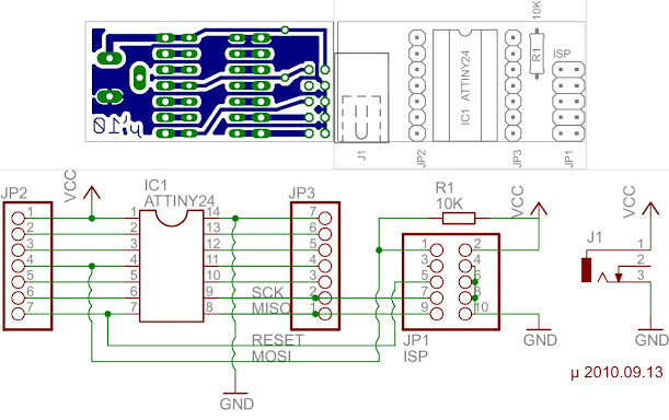
The board is single sided, with the foil on the bottom and the components on top.
(from left to right)
J1 is the power connector, with the center pin (top most) positive.
JP2 and JP3 are breakouts linked to each pin of the chip.
IC1 is the ATTINY24
R1 is a 10K resistor pulling MOSI/IC1.Pin4 up (to VCC).
JP1 is the ISP (in circuit programmer) orientated with pin 1 on top.

On the bottom of the board µ`10 has been printed to verify that the pcb is not mirrored backwards/upside down (It happens to my colleagues far more often than they'd like to admit, and we all have more than one degree!)
A ground pane has also been added to minimize the use of etchant while developing.

The PDF has been deliberately made smaller than a sheet of paper so that 'automatic-scaling' does not screw a toner/film transfer to PCB. Make certain that there is no additional scaling. The bottom layer will print pre-mirrored for toner/film transfer.

Sorry about the choice of file host; it's free but the client is really bad on memory leaks, this little 47K zip balooned to 314MB for some inexplicable reason.

Also, tell me if this design is too compact to for you, I am trying to break my bad habits of intersecting components (ie: resistor under the chip between the rows of the socket), or putting components too close for most people to populate the board (ie: IC's less than 0.1" apart).

EDIT: picture inserted

User avatar
blaze3927
Portablizer
Posts:1114
Joined:Mon Dec 08, 2008 6:14 am
360 GamerTag:notjames
Location:Australia
Contact:

Re: Getting started with diy PCB's

Post by blaze3927 » Tue Sep 14, 2010 4:02 pm

Wow thanks very much,
It looks great, ill print it today and get it on the laser photocopier tomorrow.
and megaupload is fine, i havent had any trouble with them since 05 xD.

just out of interest how lown did it take you (obviiously an experienced eagle user) to draw that up?
I'm guessing you have an engineering degree or something?
Australian Kaillera server
[url]hhttp://i56.tinypic.com/ncb0wi.gif[/url]

Snow_Cat
Posts:463
Joined:Fri Aug 13, 2010 12:40 pm
Steam ID:Snow_Cat
Location:Here
Contact:

Re: Getting started with diy PCB's

Post by Snow_Cat » Wed Sep 15, 2010 12:18 am

My pleasue;
Having things I can get done is theraputic when I've been working on some designs for years.
It took less than an hour to draw, longer to upload. But I've been using some form of CAD software every day since the early 90's, and have only started occasionally pushing content to the internet in the last couple of years.

Yes, I have two diplomas, a couple years of experience, and less than a month from completing a degree in electronics. Though I started off in software.


Remember to 'double check' the printout by laying the parts directly on the printout. (unless you are using a projector) they must line up.


Alt: use vector board and lots of wires.

User avatar
blaze3927
Portablizer
Posts:1114
Joined:Mon Dec 08, 2008 6:14 am
360 GamerTag:notjames
Location:Australia
Contact:

Re: Getting started with diy PCB's

Post by blaze3927 » Wed Oct 13, 2010 11:10 pm

long time no update :O
well after all the work snow cat put it, it turns out the pcb draw up was wrong (not snowcat's the original authors :\)
for more woes heres the other boards page:
http://nfggames.com/forum2/index.php?topic=3574.80
that problem has seem to have damaged five attiny's and 2 controllers. oh well.
I ended up having to buy a breakout board for the attinies as it was cheaper to go for the smaller 150mil revision.

Next Diy pcb:
ps2 to psp controller
Image

Uploaded with ImageShack.us

im going to spend the next few weeks navigating and learning Eagle to draw up a pcb for that.
Australian Kaillera server
[url]hhttp://i56.tinypic.com/ncb0wi.gif[/url]

Post Reply